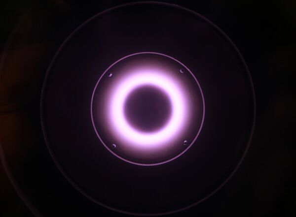
Deposition by magnetron sputtering is widely used for metallic and dielectric coatings in electronics, machine-building, architecture and other areas. For instance, deposition by magnetron sputtering is the only method of applying energy-saving coatings on the glass panes of buildings. This method is also used to apply hard coatings to cutting instruments and in all kinds of decorative coverings (titanium nitride is put on church cupolas instead of gold). In microelectronics this method is used for metallizing IC panels and in optics to make light filters.

The discovery of high-intensity pulsed magnetron discharge by MEPhI in the late 1980s was a powerful impetus for research in this field. In the 2000s Europe and the United States introduced HiPIMS (High Power Impulse Magnetron Sputtering) technology on its basis.
"However, magnetron deposition had long had a drawback — the speed at which coatings formed on materials was low compared to vacuum evaporation," RIA was told by Alexander Tumarkin, an engineer at NRNU MEPhI. He added that the coatings left by vacuum evaporation were much worse than those produced by magnetron deposition. Tumarkin said industrialists have always faced a choice between the quality of products and productivity of an enterprise. "The new device for creating a high-intensity pulsed magnetron discharge with a melted cathode combines the advantages of both methods," he said, adding that high-current sputtering of a melted target has enormous technological potential.
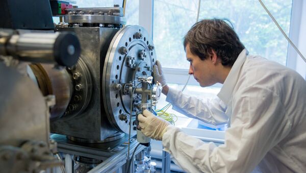
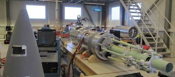
At present experts are working on prototypes of the device that will be produced on a commercial scale in the future. "The industrial prototype of the device may be used as a plasma generator in industrial and laboratory conditions as a separate module for creating high-quality films," NRNU MEPhI engineer Andrei Kaziyev said. He added that it will be required by companies producing energy-saving glass, modern energy elements and various machine-building enterprises.


