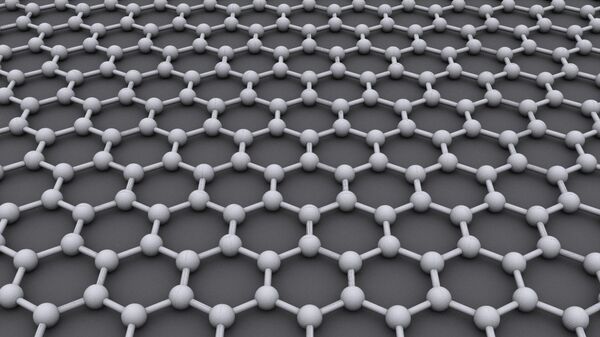
The experiments were conducted by physicists from NUST MISIS in a collaborative effort with their colleagues from the University of Helsinki and Aalto University (Finland), the University of Nottingham (Great Britain), the University of Duisburg-Essen (Germany), the University of Vienna (Austria), the Center of Research on Ions, Materials and Photonics CIMAP (France), Rugger Boskovic Institute and the Institute of Ion Beam Physics and Materials Research (Germany).
Bombarding graphene with a wide array of ions of varying mass of the elements C, O, Si, I, Au, Ta, Xe with high energies (up to 91 MeV) revealed that by changing the energy of ions it is possible to obtain nanopores in graphene with diameters ranging from one to four nanometers. The insight gained into the relationship between nanopores and ion energy brings the researchers closer to the controlled production of such structures.
"Current graphene research is looking into the possibility of changing its properties in a controlled way, such as by introducing defects into its structure," Arkady Krasheninnikov, visiting professor at NUST MISIS, said. "The creation of defects in graphene may significantly change its electronic and conductive properties and even lead to magnetism induction. Bombarding graphene with ions of various elements is one way to introduce defects into its structure. One can expect that with a regular arrangement of pores in graphene, its spectrum will change and it will become a semiconductor, which will make it usable in the electronics industry."
Researchers have been interested in porous graphene for a long time. They believe that the resulting nanostructures can be widely used in various fields of research and technology, such as purifying liquids and DNA sequencing, to name a few.


