https://sputnikglobe.com/20250324/the-first-russian-photolithographer-with-a-350-nanometer-resolution-will-be-released-in-moscow-1121678807.html
The First Russian Photolithographer With a 350-Nanometer Resolution Will Be Released in Moscow
The First Russian Photolithographer With a 350-Nanometer Resolution Will Be Released in Moscow
Sputnik International
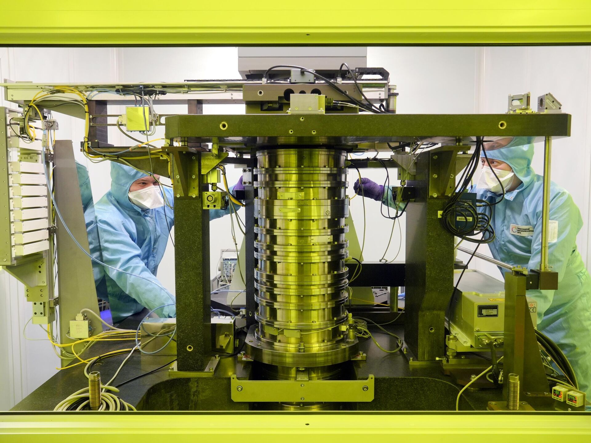
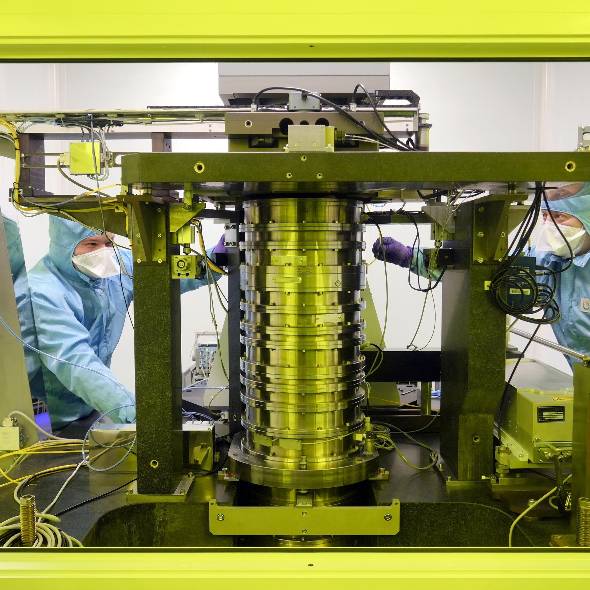
The Moscow company "Zelenograd Nanotechnology Center" has completed the development of the first Russian photolithographer with a resolution of 350 nanometers. This equipment is key in semiconductor production, Moscow Mayor Sergei Sobyanin reported on his Telegram channel.
2025-03-24T12:09+0000
2025-03-24T12:09+0000
2025-03-24T12:10+0000
russia
sergei sobyanin
moscow
russia
zelenograd
moscow government
https://cdn1.img.sputnikglobe.com/img/07e9/03/18/1121678652_0:257:2730:1793_1920x0_80_0_0_48f3e150bd20bf57dacc978b37b53634.jpg
"There are fewer than 10 countries in the world capable of creating this critical equipment for semiconductor manufacturing. Now, Russia is among them. This is a crucial step toward transitioning to domestic microelectronics production and achieving complete technological independence for the country," Sobyanin wrote.The Mayor noted that the Russian system is significantly different from foreign counterparts. For the first time, a solid-state laser—powerful, energy-efficient, and with a longer lifespan and a narrower spectrum—has been used as the light source, instead of a mercury lamp."Our company has completed the creation of the first Russian projection lithography system with a topology of 350 nanometers in accordance with a state contract. The project was implemented in partnership with the Belarusian plant 'Planar.' In December 2024, after successful tests, the equipment was accepted by the state commission, which confirmed all the stated technical specifications. There is already a customer for the equipment, and work is underway to adapt the technological processes of the system to the production features of the final consumer," explained Anatoly Kovalev, CEO of the "Zelenograd Nanotechnology Center."The photolithographer has been created for the modernization of existing and equipping new microelectronics productions to manufacture specific class products, for example, in the fields of power electronics and photonics. It features a significantly increased working field area of 22x22 millimeters, and the maximum diameter of processed wafers is 200 millimeters.As noted by the Department of Investment and Industrial Policy of Moscow, the lithographic equipment of the "Zelenograd Nanotechnology Center," which is a resident of the special economic zone "Technopolis Moscow," is in high demand for the production of a wide range of microelectronics products, including those for the automotive, aerospace, industrial automation, and consumer electronics industries.The new product from the resident of Moscow's special economic zone is already ready for mass production. Additionally, the "Zelenograd Nanotechnology Center" is continuing its work under the second state contract for the creation of a photolithographer with a resolution of 130 nanometers. The work is expected to be completed by 2026."Moscow is the center of Russian microelectronics development. Today, Moscow accounts for about 40% of the total revenue of microelectronics companies in Russia. The development of microelectronics and photonics has promising areas of application across various sectors of both the urban and commercial industries. These include optical communications, sensors, radio-photonics, and much more. Resident companies of the 'Technopolis Moscow' special economic zone are currently implementing a number of large projects, each focused on the production of strategically important products," commented Anatoly Garbuzov, Minister of the Moscow Government and Head of the Department of Investment and Industrial Policy.
https://sputnikglobe.com/20241209/russian-scientists-develop-new-energy-conservation-technique--1121110875.html
moscow
russia
zelenograd
Sputnik International
feedback@sputniknews.com
+74956456601
MIA „Rossiya Segodnya“
2025
Sputnik International
feedback@sputniknews.com
+74956456601
MIA „Rossiya Segodnya“
News
en_EN
Sputnik International
feedback@sputniknews.com
+74956456601
MIA „Rossiya Segodnya“
Sputnik International
feedback@sputniknews.com
+74956456601
MIA „Rossiya Segodnya“
first russian photolithographer, 350-nanometer resolution, moscow mayor sergei sobyanin
first russian photolithographer, 350-nanometer resolution, moscow mayor sergei sobyanin
The First Russian Photolithographer With a 350-Nanometer Resolution Will Be Released in Moscow
12:09 GMT 24.03.2025 (Updated: 12:10 GMT 24.03.2025) The Moscow company "Zelenograd Nanotechnology Center" has completed the development of the first Russian photolithographer with a resolution of 350 nanometers. This equipment is key in semiconductor production, Moscow Mayor Sergei Sobyanin reported on his Telegram channel.
"There are fewer than 10 countries in the world capable of creating this critical equipment for semiconductor manufacturing. Now, Russia is among them. This is a crucial step toward transitioning to domestic microelectronics production and achieving complete technological independence for the country," Sobyanin wrote.
The Mayor noted that the Russian system is significantly different from foreign counterparts. For the first time, a solid-state laser—powerful, energy-efficient, and with a longer lifespan and a narrower spectrum—has been used as the light source, instead of a mercury lamp.
"Our company has completed the creation of the first Russian projection lithography system with a topology of 350 nanometers in accordance with a state contract. The project was implemented in partnership with the Belarusian plant 'Planar.' In December 2024, after successful tests, the equipment was accepted by the state commission, which confirmed all the stated technical specifications. There is already a customer for the equipment, and work is underway to adapt the technological processes of the system to the production features of the final consumer," explained Anatoly Kovalev, CEO of the "Zelenograd Nanotechnology Center."
The photolithographer has been created for the modernization of existing and equipping new microelectronics productions to manufacture specific class products, for example, in the fields of power electronics and photonics. It features a significantly increased working field area of 22x22 millimeters, and the maximum diameter of processed wafers is 200 millimeters.
As noted by the Department of Investment and Industrial Policy of Moscow, the lithographic equipment of the "Zelenograd Nanotechnology Center," which is a resident of the special economic zone "Technopolis Moscow," is in high demand for the production of a wide range of
microelectronics products, including those for the automotive, aerospace, industrial automation, and consumer electronics industries.
The new product from the resident of Moscow's special economic zone is already ready for mass production. Additionally, the "Zelenograd Nanotechnology Center" is continuing its work under the second state contract for the creation of a photolithographer with a resolution of 130 nanometers. The work is expected to be completed by 2026.
"Moscow is the center of Russian microelectronics development. Today, Moscow accounts for about 40% of the total revenue of microelectronics companies in Russia. The development of microelectronics and photonics has promising areas of application across various sectors of both the urban and commercial industries. These include optical communications, sensors, radio-photonics, and much more. Resident companies of the 'Technopolis Moscow' special economic zone are currently implementing a number of large projects, each focused on the production of strategically important products," commented Anatoly Garbuzov, Minister of the Moscow Government and Head of the Department of Investment and Industrial Policy.

9 December 2024, 03:15 GMT


